A Diode is a Semiconductor (SC) device that acts as a one-way switch for the current. It allows current to flow in one direction but restricts current from flowing in the opposite direction.

 |
| Various configurations of Diodes. From left: metal case, stud mount, plastic case with band, plastic case with chamfer, glass case. |
Diode's polarity is determined by an ANODE (positive terminal) and CATHODE (negative terminal). It allows the current to flow only when the positive voltage is applied to the anode.

Whenever it allows current flow, it is called forward-biased. It is called reverse-biased when it does not permit current to flow and acts as an insulator.
The arrow of the diode's symbol considers the direction of the current flow. Because the flow of the electron considers opposite to the direction of the current.
P-N Junction Diode
If we combine the 2 types of semi-conductors P-type and N-type together, a new device is formed called a P-N junction diode. Since a junction forms between a P-type and N-type material, it is called a P-N junction.
Word diode explained as ‘Di’ means 2 and ‘ode’ means is obtained from electrode. As the formed component has 2 terminals or electrodes (one connected to P-type and the other connected to the N-type) it is called a diode or P-N junction diode or semiconductor diode.
The terminal is connected to the P-type material is known as an Anode and the terminal connected to the N-type material is called Cathode.
Junction Formation
When both the P-type and N-Type materials are joined together, (without any external voltage applied) the excess electrons in the N-type and the excess holes in P-type will get attracted to each other and recombined, and results in the formation of immobile ions (Donor ion and Acceptor ion) takes place. These immobile ions oppose the flow of electrons or holes through them, which now acts as a barrier between the two materials (formation of the barrier means the immobile ions diffuses into the P and thus the N regions). The barrier is formed and is called as Depletion region. Now, the width of the depletion region depends upon the doping concentration of the material.

Unbiased P-N Junction
If the doping concentration is equal in both materials, then the immobile ions equally diffuse into both the P and N materials.
What if the doping concentration differs with each other?
Well, if the doping differs the width of the depletion region also differs. Its diffusion is more into the lightly doped region and less into the heavily doped region.
Now let’s see the behaviour of the diode when the proper voltage is applied.
A diode in Forward Bias ( VD > 0 V)
A forward bias or “ON” condition is established by applying the positive potential to the p-type material and the negative potential to the n-type material. The application of a forward-bias potential Vd will “pressure” electrons in the n-type material and holes in the p-type material to recombine with the ions near the boundary and reduce the width of the depletion region.
The resulting minority-carrier flow of electrons from the p-type material to the n-type material (and of holes from the n-type sc diode material to the p-type material) has not changed in magnitude (since the conduction level is controlled primarily by the limited number of impurities in the material), but the reduction in the width of the depletion region has resulted in a heavy majority flow across the junction.
An electron of the n-type material now “sees” a reduced barrier at the junction due to the reduced depletion region and a strong attraction for the positive potential applied to the p-type material. As the applied bias increases in magnitude, the depletion region will continue to decrease in width until a flood of electrons can pass through the junction, resulting in an exponential rise in current.
 |
Forward-biased p–n junction: (a) internal distribution of charge under forward-bias
conditions; (b) forward-bias polarity and direction of the resulting currentA diode in Reverse Bias ( VD < 0 V)If an external potential of V volts is applied across the p – n junction, such that the positive terminal is connected to the n-type material and the negative terminal is connected to the p-type material. 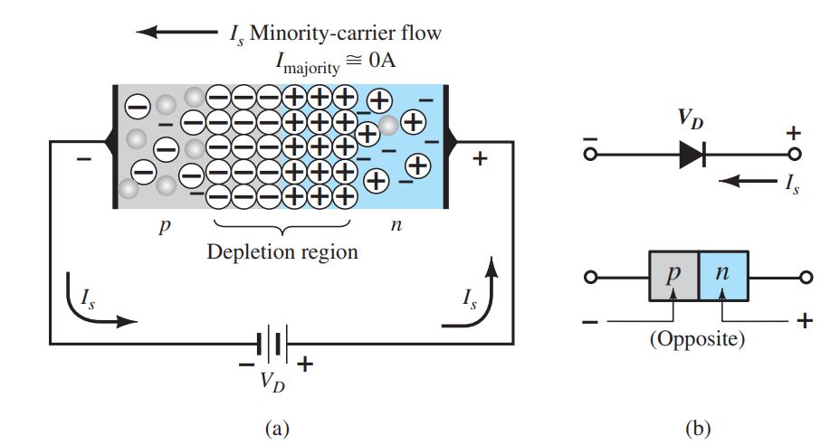 Reverse-biased p–n junction: (a) internal distribution of charge under
reverse-bias conditions; (b) reverse-bias polarity and direction of reverse
saturation current. The number (no.) of positive ions in the depletion region of the n-type material will increase due to the large no. of free electrons drawn to the positive potential of the applied voltage. For similar reasons, the no. of negative ions will increase in the p-type material. The net effect is a broadening of the depletion region. This broadening of the depletion region will establish a barrier for the majority carriers to overcome, reducing the majority carrier flow to zero. The no. of minority carriers, however, entering the depletion region will not change. The current that exists under reverse-bias conditions is also called the reverse saturation current. Types of DiodesThere are several diodes whose construction is similar but the type of material used differs. variation in diode’s properties like internal capacitance, threshold voltage etc are considered and a particular diode is designed based on those. various types of diodes with their working, symbol, and applications.
ALSO READ Definition of Electronic circuits |


0 Comments