Table of Contents --
- Electronic Device
- Advantage of Analog /Digital circuit
- Diode as a switch
- Forward/Reverse recovery time
- Storage/Transition time
Electronics Circuit
 |
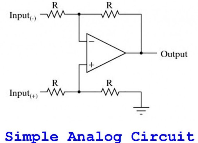
| Electronic circuit |
Electronic Device
A Device made of semiconductor material whose operation requires a controlled flow of electron
Eg- BJT, FET, Diode etc
Resistor, Inductor and capacitor are electrical devices.
Electronic Circuit are of 3 types
(1) Analog circuit (2) Digital Circuit (3) Mixed circuit
(1) Analog electronic circuit
An electronic circuit that can process analog signals or
whose input and output are analog signals.
Eg- amplifier, rectifier etc.
(2) Digital circuit

A Digital circuit processes digital signals
Eg- Decoder, counter etc
(3) Mixed-signal electronics circuit

Analog to digital and digital to analog converters are mixed signal circuits.
Advantage of digital circuits
1. Effect of noise is less.
2. Easier to design.
3. It can be programmed.
4. Digital data can be stored.
Advantage of analog circuit
- As the majority of real-time signal is analog, they can be directly processed in an analog circuit whereas digital processing requires analog to digital and digital to analog conversion.
- Analog circuits can be designed to operate even at a higher power levels.
Diode as a switch
- If a diode is in forward bias carrier crosses the junction resulting in a large flow of current therefore a diode in forward bias is considered an ON switch.
- If the diode is Reverse biased majority carrier cannot cross the junction and therefore zero current flow due to majority carriers.
- Minority carrier produces small current directed from N to P which is known as reverse current. It is equal in magnitude to reverse saturation current Io.

Hence, a diode in Reverse bias can act as an OFF switch.
- The switching speed of a diode is decided by forward and reverse recovery time.
Forward recovery time
It is time taken by a diode to change state from OFF to ON that is from reverse bias condition to forward bias condition.
Reverse recovery time
It is the time taken by a diode to change state from ON to OFF or change from forward bias condition to reverse bias condition.
practically

trr is the sum of storage time and transition time.

Storage time (ts)
- When a diode is in forward bias holes are injected into the N side and they carry a positive charge into the N side. Similarly, electrons are injected into the P side and they carry a negative charge into the P side.
- The charge carried by holes and electrons is known as an injected charge.
- An injected charge is positive on the N side and negative on the P side
- If applied voltage changes from forward bias to reverse bias the injected charge should become zero.
- For the injected charge to become zero, injected holes should become P side and injected electron should return to N side of holes and electrons should reverse their direction of the floor.
- During the reverse flow of carriers, holes and electrons recombined and disappear thus after a finite time interval injected charge becomes zero.
- The time taken by injected charge to become zero is known as storage time.
Transition time tt
- When a diode is Reverse bias transition capacitance will be present across the junction.
- The time taken by Transition capacitance to charge up to the applied reverse voltage is known as transition time tt.
- A diode fully recovers from the forward condition to reverse the condition.
1- If injected charge becomes zero in a duration ts.
2- If transition capacitance charges to applied reverse voltage in a duration tt.


i = V/ RL (If V >>
VT)
Where VT is the threshold voltage of the Diode.
- if applied voltage changes from + V to -V at t=t1 then the diode current does not immediately become zero, it rather remains equal in magnitude but changes direction because of the reverse flow of careers.
- Reverse recovery time can be reduced by decreasing ts.
- Storage time is reduced through the addition of gold as an impurity.
- Silicon and Germanium are called indirect semiconductors because the recombination process is indirect.
- In indirect recombination of an electron from conduction band first moves into an intermediate level or recombination centre present in Forbidden band and then it moves into a vacancy or for a hole in the valence band.
- Intermediate levels are allowed energy levels present in The forbidden band due to impurities are crystal imperfections.
- When gold is added as an impurity then a large number of recombination centres are created in the Forbidden band, because of that the recombination rate increase and injected charge becomes zero rapidly. Hence storage time decreases and switching speed improves.


0 Comments